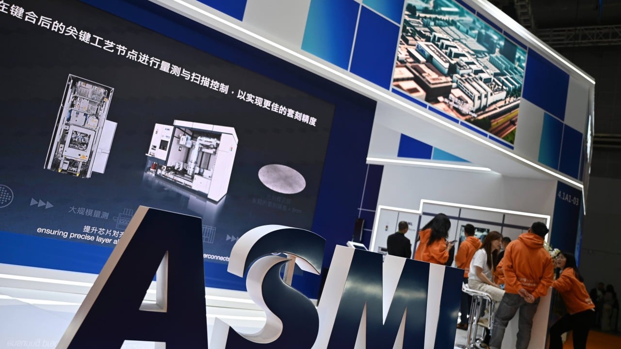
Patents don't always turn into shipping machines, yet they still move markets. When reports surfaced on ASML's patent filings around hybrid bonding, rival BE Semiconductor Industries—better known as Besi—took a hit on the stock market while ASML climbed. At the same time, Chinese chipmakers have been leaning hard into hybrid bonding to squeeze more performance out of older lithography nodes and tighter supply chains.
Put those two trends together and you see a massive shift happening right under the semiconductor industry's nose. Hybrid bonding isn't just a back-end packaging trick anymore. As transistor shrinks get harder and pricier, stacking silicon directly with copper-to-copper interconnects has become one of the most important ways to boost speed and cut power loss. You might also find this related story useful: When the Asphalt Ends and the Sky Begins.
I've watched packaging teams treat assembly like an afterthought for years. That mindset is dead. When alignment tolerances tighten to nanometers and particle counts have to stay microscopic, bonding starts looking a whole lot like front-end lithography.
What Hybrid Bonding Actually Does Differently
Old-school packaging relies on micro-bumps and solder joints to link dies together. Those bumps take up space, add resistance, and create heat bottlenecks when you stack lots of silicon vertically. As extensively documented in latest coverage by Mashable, the results are worth noting.
Hybrid bonding skips the solder gap entirely. It bonds dielectric surfaces directly and joins copper pads face-to-face at the same time. Because there's no bulky bump layer in between, signals travel shorter distances with lower energy waste and much higher interconnect density.
In practice, teams use two main flavors:
- Wafer-to-wafer bonding joins whole wafers before cutting them into individual dies. It gives high throughput and clean alignment, though you can only bond dies that match in size and layout.
- Die-to-wafer bonding places individual known-good dies onto a base wafer. That unlocks heterogeneous integration, letting engineers mix different die sizes, logic blocks, and memory chunks on one stack without wasting good silicon on bad parts.
Die-to-wafer is harder. Every single die has to be picked, checked, aligned, and bonded without tilting or picking up a speck of dust. Miss that mark and you ruin yield fast.
Why ASML's Patents Caught Everyone Off Guard
ASML built its reputation as the king of lithography—the machines that beam light through masks onto silicon wafers. Moving into hybrid bonding means stepping onto turf where Besi has been the standout volume player in die-to-wafer bonding, alongside rivals like ASMPT and EVG, and where Besi has also teamed up with Applied Materials.
According to patent analysis highlighted by SemiAnalysis and covered by Dealroom, ASML's filings point toward a track-based die-to-wafer architecture where dies ride individual carriers past process stations while a wafer meets the die for bonding. Instead of simply copying standard pick-and-place layouts, the design aims to keep stations busy and tackle the exact bottlenecks that trip up yield: alignment precision and surface cleanliness.
That makes logical sense from an engineering standpoint. Lithography lives and dies by sub-nanometer overlay and extreme contamination control. Anyone who has spent time inside a cleanroom knows how quickly a stray particle or tiny tilt ruins a bond interface—analysts have even compared surface tilt and unevenness to a wedge keeping two surfaces from mating cleanly.
Still, let's be honest: a patent is not a shipping tool. Toolmakers file hundreds of patents every year exploring ideas that never reach a customer fab floor. Moving metrology, aligning moving carriers, and keeping die-to-wafer contact clean at high speeds all carry real engineering risk. Even if ASML builds a working prototype, qualifying a new bonding tool at major logic fabs takes years of grueling yield testing.
Why Chinese Firms Are Pushing Hybrid Bonding So Hard
While ASML's patent trail grabs headlines in Europe and the U.S., Chinese semiconductor players have their own urgent reason to care about hybrid bonding. Export restrictions have tightened access to the most advanced lithography gear, forcing engineers to get creative with architecture and packaging.
If you can't easily jump straight to the newest lithography node for every part of a chip, stacking dies vertically offers a practical way to pack more compute and memory bandwidth into a tighter envelope. Industry reporting around Huawei's 9050 processor shows how aggressive partitioning—splitting logic and memory or cache layers across stacked dies—has become a real production strategy rather than just a lab experiment.
There's a catch, though. Packaging isn't a magic wand that erases transistor scaling limits forever. Stacking more layers adds thermal density, test complexity, and cost. If two dies sit on top of each other, getting heat out of the bottom layer gets trickier. Good thermal design and smart partitioning separate chips that actually ship at scale from demos that overheat on a test bench.
Logic First, Memory Later Than the Hype Suggests
A lot of hype around hybrid bonding assumes high-bandwidth memory (HBM) will switch over overnight to keep stacking higher. Not so fast.
In logic chips—like AI accelerators and high-end mobile processors—die-to-wafer hybrid bonding already has clear value because tight interconnects cut power and latency between compute and cache or partitioned logic blocks. For HBM, thermal compression bonding still has strong economics and maturity, pushing broad die-to-wafer hybrid bonding adoption in memory out toward 2029 or later unless cost and throughput math shifts dramatically.
That distinction matters if you're tracking chip stocks or planning a product roadmap. Vendor roadmaps often look smooth on a slide deck. Real fab economics are much messier.
Common Mistakes Teams Make With 3D Stacking
Having seen plenty of hardware teams chase "next-gen packaging" early, a few traps show up over and over:
- Treating bonding as a drop-in swap. You can't just take a standard 2D chip design, slap hybrid bonding on it, and expect instant wins. Floorplans, power delivery, and thermal paths have to be co-designed from day one.
- Underestimating test and known-good-die rules. In a stack, one bad die can drag down an entire multi-die assembly. Testing before bonding is non-negotiable.
- Ignoring wafer flatness and prep. Surface roughness, warpage, and contamination happen upstream during chemical-mechanical planarization and handling. Blaming the bonder alone misses half the problem.
Practical Steps If You Follow or Build in This Space
If you're an engineer, investor, or supply-chain watcher trying to separate noise from signal around hybrid bonding:
- Watch yield and throughput metrics, not just announcements. A demo bonding a few dies is easy; holding tight overlay and clean interfaces across thousands of wafers per week is what pays the bills.
- Track logic partitioning before memory hype. Look closely at how teams split SRAM, cache, or I/O from compute dies—that's where near-term commercial momentum is clearest.
- Audit thermal and supply-chain dependencies together. Pay attention to who supplies metrology, cleaning, planarization, and bonding tools, and how thermal limits constrain stack height.